System Capabilities
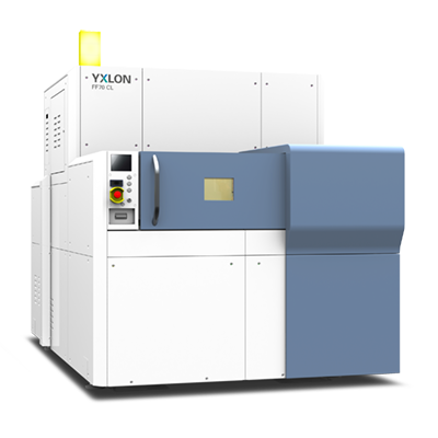
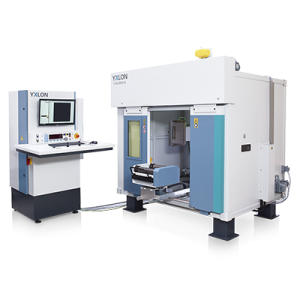
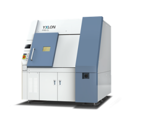
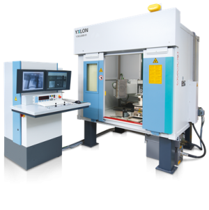
The YXLON FF70 CL is distinguished by its large inspection area of 510 x 610 mm and the extremely detail detectability of < 150 nm, making it ideal for automatically and non-destructively analyzing solder bumps and filled vias in 3D ICs, flip chips and wafers.
The innovative vacuum mechanism of the system manipulator holds the sample securely and precisely during analysis and counteracts the effects of sample warpage.
The FF70 CL provides 2D (top-down) with a high-performance flat-panel and 3D (CL-Computed Laminography) automated analysis using a high-resolution Image Intensifier within a special manipulation assembly for its inclined rotations.
The latest generation of nano-focus X-ray tubes creates 2D and 3D images that can reveal and measure the smallest voids and features. This enables the YXLON FF70 CL to analyze the most demanding advanced semiconductor challenges.
A user-friendly and intuitive graphical user interface (GUI) allows the easy creation of automated, multi-point and multi-functional analysis inspection programs.
Measurement repeatability over time is ensured by automatic, continuously monitoring background calibration tests over all aspects of the system.
System properties at a glance:
- Automated high-throughput analysis with the best reproducibility and reliability of the results
- Simple creation of automated, multi-point and multi-functional analysis inspection programs allowing rapid change between sample and measurement tasks
- Continuous background monitoring and optimization to ensure measurement repeatability and accuracy
Technical Data
| Attribute | Respective Value |
|---|---|
| Sample Diameters | 795 [mm] (30.1″) |
| Sample Height | 150 [mm] (5.7″) |
| Maximum Sample Weight | 2 [kg] |
| System Dimensions | 1940 x 2605 x 2000 [mm] |
| CT Modes | Ultra-high resolution Computed Laminography (CL) |
| Manipulation | Ultra-precise manipulator, active anti-vibration system, highest reliability |




Đánh giá
Chưa có đánh giá nào.