Static EBSD
3D Crystallographic Studies in Nano and Micro Scales
Discover grain size, crystal structure and crystal orientation of your sample surface by means of electron backscattered diffraction (EBSD). Use a FIB-SEM instrument to gain the same information in 3D. Remove sample material and analyse the cross sections in an iterative process.
Conventional 3D EBSD Experiment
In conventional 3D EBSD you have to move your sample between two stage positions:
- FIB milling position: The FIB cuts into the sample to prepare a surface for EBSD analysis.
- EBSD analysis position: The prepared surface is repositioned to face the EBSD detector.
These two operations alternate up to hundreds of times to enable 3D analysis of the volume of interest. To guarantee accurate sample positioning, image registration after every stage movement is required.
Advantages of Static 3D EBSD
The static EBSD geometry allows you to accomplish FIB material removal and EBSD analysis in the same stage position. Avoid stage movements and image registration steps. Increase your throughput and 3D EBSD data quality.
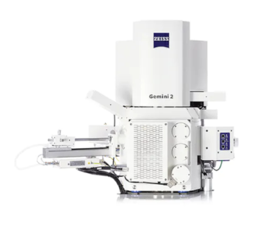
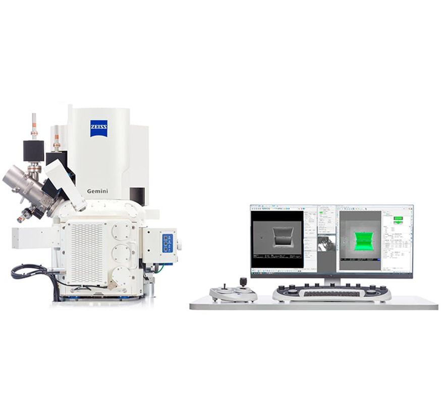
In collaboration with LEM3, Université de Lorraine, Metz, France, and Bruker Nano GmbH, ZEISS has customized an Auriga instrument to realize the static EBSD geometry.
Analytical Chamber
ZEISS Merlin provides superb image resolution for high probe currents. With a current stability of better than 0.2%/h, it is your tool of choice for analytical applications.
A new chamber design for the Merlin Series supports the use of a fully focusing WDS spectrometer from Oxford Instruments. The result is an ideal geometry for simultaneous acquisition of EDS, EBSD and WDS data.
All three analytical detectors are mounted on the same side of the chamber with an analytical working distance of 8.5mm. As an option you can use a charge compensation unit during sample analysis to characterize non-conductive samples.
SIMS
In a FIB-SEM instrument, secondary ion mass spectrometry (SIMS) is used to detect atomic ions or ionized molecules which have been sputtered from the sample using the Ga+ FIB. The detected ions originate from the upper monolayers of the sample. They carry analytical information.
Use SIMS to analyse trace elements down to ppm level in thin films, semiconductors or solar cells. Detect different isotopes of the same element and achieve an analytical spatial resolution of down to 50nm.
In the past, Auriga, Auriga Compact, and Auriga 60 systems have been successfully customized with a SIMS detector from Hiden Analytical Ltd.
Cryo
The cryogenic (cryo) equipment allows studies of wet samples under high vacuum conditions in the scanning electron microscope. Prior to their transfer into the electron microscope, the samples are shock frozen. During transfer and study in the microscope the sample is always kept at very low temperatures, typically around -140°C.
All ZEISS electron microscopes are compatible with cryo systems from the manufacturers Quorum Technologies Ltd., Leica Microsystems GmbH, and Gatan Inc., which are the most popular cryo systems in the market.
A cryo system is characterized by three components:
- cryo stage
- cryo shield
- cryo airlock
The cryo shield acts as a cold trap and is customized to achieve the biggest possible surface – compatible with stage motion and tool configuration.
In-situ Experiments
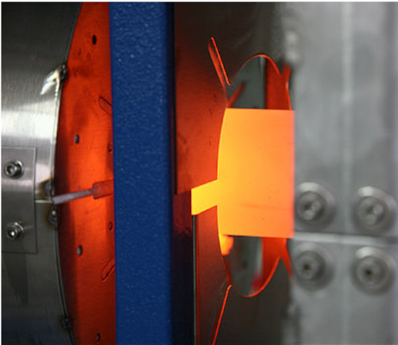
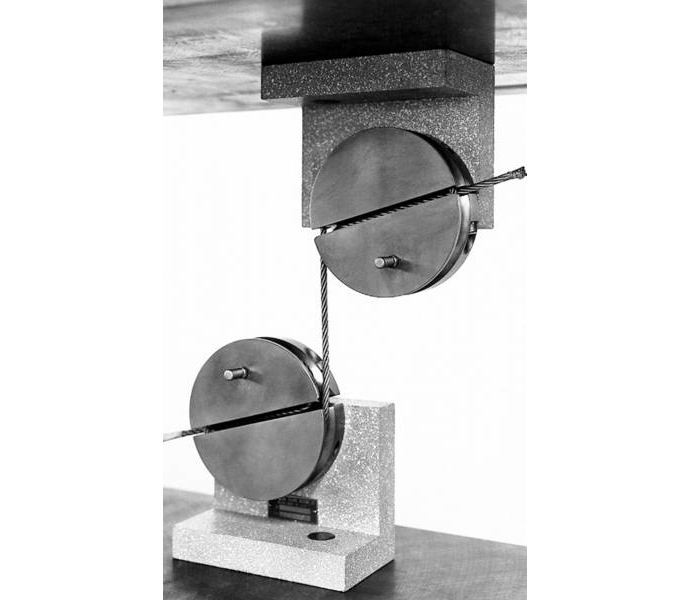
Tensile and heating stages are useful tools in materials research. They allow in-situ mechanical testing and/or heating of samples under SEM observation. Dynamic studies of the sample morphology and crystallographic structure as a function of load or temperature are possible.
Heating stages are available with maximum temperatures from 300°C up to 1500°C.
Tensile stages provide a maximum sample load from 200N up to 5000 N.
The planning of your experiment also depends on maximum sample weight and size.
Hot Cell
In nuclear industry and nuclear research ZEISS electron microscopes are used in radiation shielded environments, or Hot Cells.
In a Hot Cell, heavy metal alloy outer shielding protects operators and people from radiation. Glove boxes avoid nuclear contamination of the environment. Automatism and remote microscope operation improve safety. Sensitive electronic devices and detectors are protected from gamma and beta radiation by means of static or movable shields.
The customization of ZEISS electron microscopes for Hot Cell applications is done in close collaboration with our partner Défi Systèmes (Nîmes, France).



Đánh giá
Chưa có đánh giá nào.