


Highlights

Maximize Your SEM Insights
Take advantage of achieving up to 30% better SEM resolution at low voltage.
- Count on the SEM performance of your ZEISS Crossbeam for 2D surface sensitive images or when performing 3D tomography
- Benefit from high resolution, contrast and signal-to-noise ratios, even when using very low accelerating voltages
- Characterize your sample comprehensively with a range of detectors. Get pure materials contrast with the unique Inlens EsB detector
- Investigate non-conductive specimens undisturbed by charging artifacts.

Increase Your FIB Sample Throughput
Profit from up to 40% faster material removal by the introduction of intelligent FIB milling strategies.
- Use the gallium FIB column Ion-sculptor for a new way of FIB-processing
- Get high quality samples, minimize FIB-induced damage and perform experiments faster at the same time
- Manipulate your samples precisely and fast by using up to 100 nA current without compromising FIB resolution
- Profit from speed and precision of intelligent FIB scanning strategies for material removal and perform your experiments up to 40% faster than before

Experience Best 3D Resolution in Your FIB-SEM Analysis
Enjoy the benefits of integrated 3D analysis for EDS and EBSD investigations.
- Expand the capacity of your Crossbeam with ZEISS Atlas 5, the market-leading package for fast, precise tomography
- Perform EDS and EBSD analysis during tomography runs with the integrated 3D Analytics module of ZEISS Atlas 5
- Profit from best 3D resolution and leading isotropic voxel size in FIB-SEM tomography. Probe less than 3 nm in depth and produce surface sensitive, material contrast images using the Inlens EsB detector
- Save time by collecting your serial section images while milling. Take advantage of trackable voxel sizes and automated routines for active control of image quality
ZEISS Crossbeam Laser Workflow
How the LaserFIB Workflow Enhances Your in situ Studies
For in situ studies you need to localize ROIs in 3D, ablate material via a targeted preparation and perform 3D imaging and analytics. Add a femtosecond laser to your ZEISS Crossbeam and benefit from ultra-fast sample preparation.

- Gain rapid access to deeply buried structures
- Prepare extremely large cross-sections up to millimeters in width and depth
- Benefit from minimal damage and heat affected zones due to ultrashort laser pulses
- Perform laser work in a dedicated chamber to avoid contamination of your FIB-SEM
- Find your hidden ROIs by correlation with previously acquired X-ray microscopy datasets
The Workflow for TEM Lamella Preparation
Just do it with high quality at high throughput


3. Lift out
- Bring in the micromanipulator and attach the lamella to its tip
- Cut out the lamella from the bulk
- The lamella is then ready for lift out and can be transferred to a TEM grid

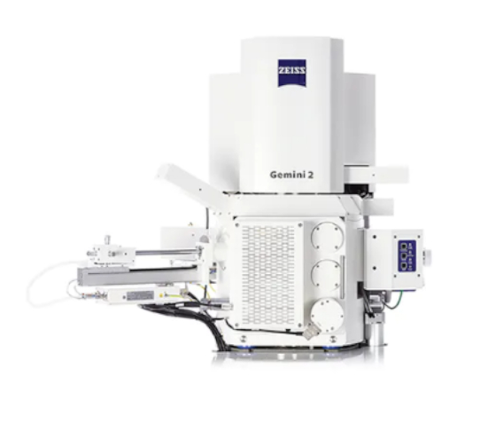
SEM Electron Optics
Choose between Two Columns
The FE-SEM column of ZEISS Crossbeams is based on Gemini electron optics as all ZEISS FE-SEMs. Decide on the Gemini VP column of Crossbeam 350 or the Gemini II column of Crossbeam 550.
Field emission SEMs are designed for high resolution imaging. Key to the performance of a field emission SEM is its electron optical column. Gemini technology comes with all ZEISS FE-SEMs and FIB-SEMs: it is tailored for excellent resolution on any sample, especially at low accelerating voltages, for complete and efficient detection, and ease-of-use.
Gemini Optics is Characterized by Three Main Components
- The Gemini objective lens design combines electrostatic and magnetic fields to maximize optical performance while reducing field influences at the sample to a minimum. This enables excellent imaging, even on challenging samples such as magnetic materials.
- Gemini beam booster technology, an integrated beam deceleration, guarantees small probe sizes and high signal-to-noise ratios.
- The Gemini Inlens detection concept ensures efficient signal detection by detecting secondary (SE) and backscattered (BSE) electrons in parallel minimizing time-to-image.
Benefits for Your FIB-SEM Applications
- Long-term stability of the SEM alignment and the effortless way it adjusts all system parameters such as probe current and acceleration voltage
- Achieve distortion-free, high resolution imaging even over large fields of view with the help of the near magnetic-field free optics
- Tilt the specimen without influencing the electron optical performance


Crossbeam 350 with Gemini I VP
- Maximum sample flexibility in multi-purpose environments
- In situ experiments with outgassing or charging samples
- Unique Gemini material contrast with the Inlens EsB detector
Crossbeam 550 with Gemini II
- High resolution even at low voltage and high current thanks to the double condenser system
- More information in less time with high resolution imaging and fast analytics
- Unique topographical and material contrast with simultaneous Inlens SE and EsB imaging
Gemini Novel Optics
Profit from Surface Sensitive Imaging
High resolution imaging at low landing energy is required for beam as a standard. It is essential for:
- beam sensitive samples
- non-conductive materials
- gaining true sample surface information without undesirable background signal from deeper sample layers
The novel Gemini optics are optimized for resolutions at low and very low voltages and for contrast enhancement.
Technological characteristics are the high gun resolution mode and the optional Tandem decel.
- The high gun resolution mode results in minimized chromatic aberration thanks to of a reduction of primary energy width by 30%.

Tandem decel, now introduced to ZEISS Crossbeam 350/550, can be used in two different modes:
- Tandem decel, a two-step deceleration mode, combines the beam booster technology with a high negative bias voltage that is applied to the sample: the electrons of the primary electron beam are decelerated, thus the landing energy is effectively reduced
- Apply a variable negative bias voltage between 50 V and 100 V. One application mode enhances the contrast of your images
- Apply a negative bias voltage between 1 kV and 5 kV and improve the low kV resolution of your images
FIB-SEM Technology
Discover a new way of FIB processing
The Ion-sculptor FIB column speeds up your FIB work without compromising machining precision and lets you benefit of its low voltage performance for any sample.

The ZEISS Crossbeam Family carries the next-generation focused ion beam column, Ion-sculptor, featuring high currents for high throughput and excellent low voltage performance for high sample quality.
- Maximize sample quality by using the low voltage capabilities of the Ion-sculptor FIB column
- Minimize amorphization of your specimens and get the best results after thinning
- Get precise and reproducible results with maximum stability
- Accelerate your FIB applications with fast probe current exchanges
- Perform high throughput experiments thanks to beam currents of up to 100 nA
- Achieve exceptional FIB resolution of less than 3 nm
- The Crossbeam family comes with automatic FIB emission recovery for long-term experiment
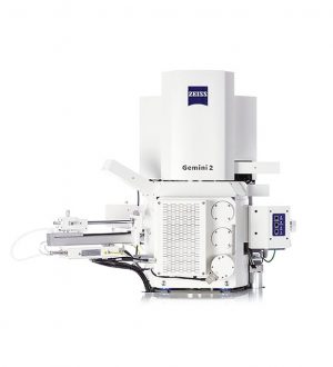
ZEISS Crossbeam Family
Within ZEISS Crossbeam Family you have the choice between Crossbeam 350 or Crossbeam 550. Exploit the variable pressure capabilities of Crossbeam 350 (optional). Or use Crossbeam 550 for your most demanding characterizations and choose the chamber size, standard or large, that best suits your samples.
| ZEISS Crossbeam 350 | ZEISS Crossbeam 550 | |
| SEM | Gemini I optics VP option Tandem decel option | Gemini II optics – Tandem decel option |
| Chamber Size and Ports | Standard with 18 configurable ports | Standard with 18 configurable ports or large with 22 configurable ports |
| Stage | 100 mm travel range in x/y | Standard with 100 mm or large 153 mm travel range in x/y |
| Charge Control | Flood Gun Local Charge Compensation Variable Pressure | Flood Gun Local Charge Compensation – |
| Exemplified Options | Inlens SE and Inlens EsB* for simultaneous imaging SE/EsB* imaging VPSE detector | Inlens SE and Inlens EsB* for simultaneous imaging SE/EsB* imaging large airlock for 8 inch wafersconfigure three pneumatically driven accessories simultaneously on the large chamber, e.g. STEM, 4-Quadrant-Backscatter detector, and local charge compensation |
| Advantages | Maximum sample variety due to optional variable pressure mode, wide range of in situ experiments, sequential Inlens SE / EsB* imaging possible. | High throughput in analytics and imaging, high resolution under all conditions, simultaneous Inlens SE and Inlens EsB* imaging |
| * SE secondary electron, EsB energy selective backscatter |


Đánh giá
Chưa có đánh giá nào.