material-testing.com.vn
  • Home
  • About Us
  • Products
    • Material testing machineMaterial testing machine
      • Abrasion testing machineAbrasion testing machine
      • Bending testing machineBending testing machine
      • Compression testing machine
      • Folding endurance testing machineFolding endurance testing machine
      • Impact testing machineImpact testing machine
      • PlastimeterPlastimeter
      • Torsion testing machineTorsion testing machine
      • Universal testing machineUniversal testing machine
      • Melt FlowMelt Flow
      • Hardness testerHardness tester
    • MicroscopesMicroscopes
      • 3D optical microscope3D optical microscope
      • 3D X-ray Microscopy3D X-ray Microscopy
      • Atomic force microscopeAtomic force microscope
      • Digital microscopesDigital microscopes
      • Fluorescence MicroscopesFluorescence Microscopes
      • Inverted material science microscopesInverted material science microscopes
      • Measuring microscopesMeasuring microscopes
      • Portable metallographic microscopesPortable metallographic microscopes
      • Stereo microscopesStereo microscopes
      • Upright material science microscopesUpright material science microscopes
    • Elemental analysis equipmentElemental analysis equipment
      • Handheld analyzersHandheld analyzers
      • SpectroscopeSpectroscope
      • X-ray DiffractometerX-ray Diffractometer
    • NDTNDT
      • Magnetic particle imagingMagnetic particle imaging
      • Microscopy cameraMicroscopy camera
      • Tomography equipmentTomography equipment
      • Ultrasonic inspectionUltrasonic inspection
      • X-ray and CT Inspection systemsX-ray and CT Inspection systems
    • High Therm equipmentHigh Therm equipment
      • Induction heatingInduction heating
      • Microwave heatingMicrowave heating
      • Resistance heatingResistance heating
    • Biological equipmentBiological equipment
      • Kit
    • Signal analyzerSignal analyzer
      • Audio analyzerAudio analyzer
      • Network analyzerNetwork analyzer
      • Radio analyzerRadio analyzer
      • Video and image analyzerVideo and image analyzer
    • Semiconductor metrology equipmentSemiconductor metrology equipment
    • Environmental test chambersEnvironmental test chambers
    • Sample preparation equipmentSample preparation equipment
    • AccessoriesAccessories
  • Testing
    • Torsion
    • Compression
    • Flexure
    • Impact
    • Tensile
    • Friction
    • Bending
    • Hardness
    • Micro
    • Surface
    • Elemental Analysis
    • Plasticity
    • Scan
    • Signal Analysis
  • Materials
    • Wood
    • Textiles Materials
    • Stones
    • Signal
    • Rubbers
    • Plastics
    • Metal
    • Medical Materials
    • Composite
    • Components Parts
    • Biomaterials
    • Alloy
    • Adhesive Materials
  • Manufacturer
    • Tinius Olsen
    • GBC
    • Prescott
    • Bruker
    • EchoLAB
    • EchoENG
    • Angelatoni
    • LTF
    • Linn High Therm
    • Data Physic
    • Tektronics
    • Elvatech
    • Yxlon
  • News
  • Contact
  • English
    • Tiếng Việt
    • English
Twitter Email YouTube linkedin
Menu
material-testing.com.vn
Facebook Twitter Google Email Pinterest
HomeMicroscopesScanning Electron & Ion Microscopes GeminiSEM Family

GeminiSEM Family

For the Highest Demands in Imaging and Analytics from Any Sample

The GeminiSEM family stands for effortless imaging with sub-nanometer resolution and high detection efficiency, even in variable pressure mode. Rely on surface sensitive imaging and analytics and profit from the highest sample flexibility. Choose a flexible and reliable field emission scanning electron microscope (FESEM) for your research in materials science or life sciences, your industrial lab or in an imaging facility.

With the GeminiSEM family you will always get excellent images and reliable analyses from any real-world sample.
  • GeminiSEM 500 brings you more signal and more detail, especially at very low voltages. Its variable pressure mode makes you feel like you’re working in high vacuum.
  • GeminiSEM 450 is your specialist for speed and surface sensitivity. Profit from ease-of-use by design and flexibility for imaging and analytics.
  • GeminiSEM 300 lets you experience high resolution and high contrast even on extremely large fields of view. Especially, but not solely, liked by novice users at high or low vacuum.
Manufacturer

Zeiss

Testing

Micro

 
  • Description
  • Reviews (0)
Description

Highlights

The Family

Image any of your samples effortlessly at sub-nanometer resolution and high detection efficiency. Rely on surface sensitive analysis. Capitalize on variable pressure. Profit from the highest sample flexibility.

GeminiSEM - Crisp Image

More Signal and More Detail

GeminiSEM 500 brings you more signal and more detail, especially at very low voltages for any sample. Acquire crisp images fast and with minimum sample damage.
  • Acquire crisp images fast and with minimum sample damage thanks to significantly increased Inlens detection signal.
  • Resolve nanoscale details with high resolution and contrast at low voltages and profit from perfect image quality, without requiring sample bias.
  • At 500 V you can resolve 1.0 nm with perfect image quality, without requiring beam deceleration.
  • Apply beam deceleration, Tandem decel, and achieve even up to 0.8 nm at 1 kV.
  • The new variable pressure mode, NanoVP, makes you feel like you’re working in high vacuum.
GeminiSEM - EBSD Coin

Speed and Surface Sensitivity for Both Imaging and Analytics

GeminiSEM 450 is your specialist for speed and surface sensitivity in imaging and analytics. Achieve spatial resolution during EDS or EBSD experiments easy and fast.
  • Take advantage of high resolution and surface sensitivity for your EDS or EBSD analysis, especially when working with low voltages.
  • Image large areas of your sample fast and with excellent quality
  • Profit from the optical design: you do not lose time in complicated realignments as you work.
  • Investigate non-conductive, or magnetic or any kind of sample: Work in high vacuum or variable pressure – no need for compromise either, whether on the speed or the quality of your images and analyses.
GeminiSEM - Magnetic Materials

Imaging Flexibility

GeminiSEM 300 lets you experience high resolution and high contrast even on extremely large fields of view. Especially, but not solely, liked by for novice users at high or low vacuum.
  • Image large fields of view with excellent image quality and fast-time-to-image.
  • Count on efficient detection, excellent resolution and distortion-free, large area images.
  • Profit from the novel optical design’s high gun resolution mode that is tailored to low voltage imaging even for challenging samples, such as beam-sensitive or magnetic materials.
  • Characterize your sample comprehensively: obtain unique low voltage, material contrast with the energy selective backscatter detector.
  • Utilize the NanoVP mode: Image non-conductive specimens at high resolution with excellent surface sensitivity with the Inlens SE detector at higher pressures.
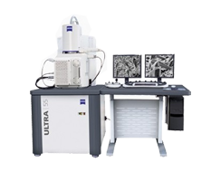
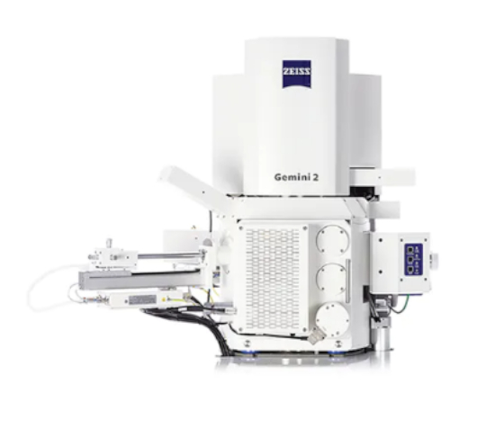
 

Essential Specifications 

ZEISS GeminiSEM 500


ZEISS GeminiSEM 450


ZEISS GeminiSEM 300


Thermal field emission type, stability better than 0.2 %/h
Acceleration Voltage0.02 – 30 kV
Probe Current3 pA – 20 nA3 pA – 40 nA3 pA – 20 nA
(100 nA configuration also available)(100 nA or 300 nA configuration
also available)


(100 nA configuration also available)
Store Resolution

Up to 32k × 24k pixels

Magnification
50 – 2,000,000
12 – 2,000,000
12 – 2,000,000
Detectors available in basic configuration
Inlens Secondary Electron detector
Everhart Thornley Secondary Electron
detector
High efficiency VPSE detector
(included in variable pressure option)
Selected OptionsInlens Energy selected Backscatter
detector (EsB)
Angular selective backscattered detectorAngular selective backscattered detector
Annular STEM detector (aSTEM 4)
EDS Detector (energy dispersive
spectroscopy)
EBSD Detector (electron backscatter
diffraction) Investigation of crystalline orientation
NanoVP
Local Charge Compensation
Additional stage options available
on request

The Technology Behind

Gemini Electron Optics


Gemini Basics


The Gemini optical column consists a beam booster, Inlens detectors and a Gemini objective

Gemini 1 – What You Always Wanted to Know about the Basics

Field emission SEMs are designed for high resolution imaging. Key to the performance of a field emission SEM is its electron optical column. Gemini is tailored for excellent resolution on any sample, especially at low accelerating voltages, for complete and efficient detection, and ease-of-use.

Gemini optics is characterized by three main components:

  • The Gemini objective lens design combines electrostatic and magnetic fields to maximize optical performance while reducing field influences at the sample to a minimum. This enables excellent imaging, even on challenging samples such as magnetic materials.
  • Gemini beam booster technology, an integrated beam deceleration, guarantees small probe sizes and high signal-to-noise ratios.
  • The Gemini Inlens detection concept ensures efficient signal detection by detecting secondary (SE) and backscattered (BSE) electrons in parallel minimizing time-to-image.

For your applications benefit from:

  • Long-term stability of the SEM alignment and the effortless way it adjusts all system parameters such as probe current and acceleration voltage.
  • Achieve distortion-free, high resolution imaging with the help of the near magnetic-field free optics.
  • Get information solely from the top-most layer of your samples with the Inlens SE detector that produces images out of the truly surface sensitive SE 1 electrons true.
  • Obtain true material contrast at very low voltages with the detection concept of the Inlens EsB detector.

Gemini 1 and its Novelties


Novel optical design of Gemini column
GeminiSEM 300 and GeminiSEM 500. High resolution gun mode, Tandem decel and Nano-twin lens as part of the novel optical design (highlighted). Nano-twin lens only available in GeminiSEM 500 (highlighted in red).

Gemini 1 Novelties – the Development Goes on

Today’s SEM applications demand high resolution imaging at low landing energy as a standard.
It is essential for:
  • Beam sensitive samples
  • Non-conductive materials
  • Gaining true sample surface information without undesirable background signal from deeper sample layers

The novel Gemini optics are optimized for resolutions at low and very low voltages and for contrast enhancement. Technological characteristics are the high gun resolution mode, GeminiSEM 500’s Nano-twin lens and the optional Tandem decel.

The high gun resolution mode results in:
  • Minimized chromatic aberration thanks to of a reduction of primary energy width by 30%
  • Allows even smaller probe sizes
The Nano-twin lens delivers:
  • Better resolution at low and ultra-low voltages by optimizing the geometry and the electrostatic and magnetic field distributions.
  • An enhanced Inlens detector signal under low voltage imaging conditions.

Tandem decel lets you maximize high resolution imaging on suitable samples:

  • Tandem decel, a two-step deceleration mode, combines the beam booster technology with a high negative bias voltage that is applied to the sample: the electrons of the primary electron beam are decelerated, thus the landing energy is effectively reduced.
  • Use this to further improve resolution below 1 kV and boost the detection efficiency of backscattered diode detectors.
  • Tandem decel optional sample biasing up to 5 kV further improves the excellent imaging capabilities at low voltages.

Gemini 2


ZEISS GeminiSEM 450: Gemini 2 column with double condenser, two Inlens detectors and NanoVP or local charge compensation

Capitalize on Gemini 2 Optics

A comprehensive characterization of any sample calls for performance in imaging and in analytics. Plus, today’s users expect the set up and handling of the instrument to be easy. The Gemini 2 optics answers these demands:
  • GeminiSEM 450 comes with Gemini 2 optics featuring a double condenser
  • Adjust the beam current continuously while the spot size stays optimized simultaneously
  • Switch seamlessly between high resolution imaging – at low beam currents – and analytical modes – at high beam currents
  • You save time and effort because there’s no need to realign the beam after changing imaging parameters
  • Stay flexible: use the highest beam current density for high resolution imaging and analysis at both low and high beam current, independently of which beam energy you select
  • Your specimen won’t exposed to a magnetic field: achieve a distortion-free EBSD patterns and high resolution imaging over a large field of view
  • Tilt the specimen without influencing the electron optical performance. Image even magnetic samples easily
  • Choose a charge reduction mode that suits your sample best: local charge compensation, variable pressure in the chamber or NanoVP

Variable Pressure


NanoVP: differential pumping aperture with insulating o-ring underneath the Gemini objective lens in the SEM chamber.

NanoVP – Get More Detail and Stay Flexible in Variable Pressure Mode

NanoVP technology offers the best way to reduce charging on non-conductive samples without compromising Inlens detection capabilities and resolution.
  • Reduce charging on non-conductive samples.
  • NanoVP technology reduces beam broadening and thus enables both imaging of high resolution details and true in-lens detection up to 150 Pa.
  • Hence, Inlens SE and EsB detectors can be used, even simultaneously, in VP mode for high resolution surface and materials contrast imaging.
  • Pressure can even be elevated up to 500 Pa using chamber VPSE detection for your most challenging samples.

Applications

ZEISS GeminiSEM


Materials Science


Precursor material for functional surface, gold nanoparticles on polystyrene sphere, imaged with GeminiSEM 500, at 3 kV.
Precursor material for functional surface, gold nanoparticles on polystyrene sphere, imaged: GeminiSEM 500 at 3 kV.
Etched silicon nanostructures at 50 V, no sample biasing. Imaged with GeminiSEM 500
Etched silicon nanostructures at 50 V, no sample biasing. Imaged with GeminiSEM 500. Sample: courtesy of A. Charai, Aix Marseille University, France.
Silica-supported Cobalt catalyst
Silica-supported Cobalt catalyst is characterized by means of high resolution imaging and EDS analysis at 25 kV using GeminiSEM 450 and Oxford Instruments Ultim Max 170 EDS detector.
Metal foams like this open cell nickel foam are widely used as cathode substrate in batteries or super-capacitors.
Fractured surface of a NdFeB magnet
Fractured surface of a NdFeB magnet.
Investigation of the fractured surface of an NdFeB magnet (demagnetized) with GeminiSEM 450.
Lithium ion battery cathode shows no beam damage of sensitive binder material at 500 V
Lithium ion battery cathode shows no beam damage of sensitive binder material at 500 V.
Lithium ion battery cathode. EDS compositional mapping shows main constituents of the different oxides
Lithium ion battery cathode. EDS compositional mapping shows main constituents of the different oxides.

Life Sciences


Moth wing, Inlens SE detector, at 50 V, in high vacuum.
Large field oBrain section, large field of view, imaged using 3View® in combination with GeminiSEM 300.f view of a brain section imaged using 3View® in combination with GeminiSEM 300.
Brain section, large field of view, imaged using 3View® in combination with GeminiSEM 300.
Cilia, imaged with the BSD detector in GeminiSEM 450.
Brain section, imaged without Tandem decel results in low contrast.
Brain section, applying Tandem decel increases contrast
Brain section, applying Tandem decel increases contrast.
T4-Phage, negative stained, imaged with a STEM detector
T4-Phage, negative stained, imaged with a STEM detector.

Semiconductor / Electronics


Data storage, hard disk read head.
Data storage, hard disk read head. Left: Inlens SE detector. Right: Inlens EsB detector.
FinFET transistor, top view, 22 nm technology.
FinFET transistor, top view, 22 nm technology, 3 kV, pure BSE imaging using EsB, high material contrast.

Industry


The magnetic grains of a hard disk platter, a magnetic data storage medium, are only a few nanometers in scale, which affects the bit density and thus the data capacity of the hard disk.
Metal foams like this open cell nickel foam are widely used as cathode substrate in batteries or super-capacitors.
NanoVP, VPSE Detector, 150Pa, 3kV. Fibrous polymer microstructures
NanoVP, VPSE Detector, 150Pa, 3kV. Fibrous polymer microstructures.
Reviews (0)

Reviews

There are no reviews yet.

Only logged in customers who have purchased this product may leave a review.

Category: Scanning Electron & Ion Microscopes
Share
Facebook Twitter Google Email Pinterest

Related products

Close

MultiSEM 505/506

Scanning Electron & Ion Microscopes
Close

Crossbeam

Scanning Electron & Ion Microscopes
Close

Sigma Family

Scanning Electron & Ion Microscopes
Close

EVO Family

Scanning Electron & Ion Microscopes
Close

Customized Tools

Scanning Electron & Ion Microscopes
Close

ORION NanoFab

Scanning Electron & Ion Microscopes

VIETNAM INTELLIGENT SERVICE AUTOMATION SOLUTIONS CO., LTD.
(VISAS CO., LTD).
Add: 6 Mac Thai To, Yen Hoa Ward, Cau Giay District, Hanoi, Vietnam.
Hotline : +84 386198984

Email    : info2@visasltd.com


Contact
close slider

    LIÊN HỆ/CONTACT


    • Home
    • About Us
    • Products
      • Material testing machineMaterial testing machine
        • Abrasion testing machineAbrasion testing machine
        • Bending testing machineBending testing machine
        • Compression testing machine
        • Folding endurance testing machineFolding endurance testing machine
        • Impact testing machineImpact testing machine
        • PlastimeterPlastimeter
        • Torsion testing machineTorsion testing machine
        • Universal testing machineUniversal testing machine
        • Melt FlowMelt Flow
        • Hardness testerHardness tester
      • MicroscopesMicroscopes
        • 3D optical microscope3D optical microscope
        • 3D X-ray Microscopy3D X-ray Microscopy
        • Atomic force microscopeAtomic force microscope
        • Digital microscopesDigital microscopes
        • Fluorescence MicroscopesFluorescence Microscopes
        • Inverted material science microscopesInverted material science microscopes
        • Measuring microscopesMeasuring microscopes
        • Portable metallographic microscopesPortable metallographic microscopes
        • Stereo microscopesStereo microscopes
        • Upright material science microscopesUpright material science microscopes
      • Elemental analysis equipmentElemental analysis equipment
        • Handheld analyzersHandheld analyzers
        • SpectroscopeSpectroscope
        • X-ray DiffractometerX-ray Diffractometer
      • NDTNDT
        • Magnetic particle imagingMagnetic particle imaging
        • Microscopy cameraMicroscopy camera
        • Tomography equipmentTomography equipment
        • Ultrasonic inspectionUltrasonic inspection
        • X-ray and CT Inspection systemsX-ray and CT Inspection systems
      • High Therm equipmentHigh Therm equipment
        • Induction heatingInduction heating
        • Microwave heatingMicrowave heating
        • Resistance heatingResistance heating
      • Biological equipmentBiological equipment
        • Kit
      • Signal analyzerSignal analyzer
        • Audio analyzerAudio analyzer
        • Network analyzerNetwork analyzer
        • Radio analyzerRadio analyzer
        • Video and image analyzerVideo and image analyzer
      • Semiconductor metrology equipmentSemiconductor metrology equipment
      • Environmental test chambersEnvironmental test chambers
      • Sample preparation equipmentSample preparation equipment
      • AccessoriesAccessories
    • Testing
      • Torsion
      • Compression
      • Flexure
      • Impact
      • Tensile
      • Friction
      • Bending
      • Hardness
      • Micro
      • Surface
      • Elemental Analysis
      • Plasticity
      • Scan
      • Signal Analysis
    • Materials
      • Wood
      • Textiles Materials
      • Stones
      • Signal
      • Rubbers
      • Plastics
      • Metal
      • Medical Materials
      • Composite
      • Components Parts
      • Biomaterials
      • Alloy
      • Adhesive Materials
    • Manufacturer
      • Tinius Olsen
      • GBC
      • Prescott
      • Bruker
      • EchoLAB
      • EchoENG
      • Angelatoni
      • LTF
      • Linn High Therm
      • Data Physic
      • Tektronics
      • Elvatech
      • Yxlon
    • News
    • Contact
    • English
      • Tiếng Việt
      • English
    Scroll To Top